04/05: #
Negative Feedback (NFB) #
- The main idea is ‘how do we get an op-amp to output a voltage that isn’t railing?’
- Negative feedback refers to the idea that there is some output amount that is the ideal or intended amount
- If the actual amount becomes larger than this reference, then the system must detect this deviation and bring it down to the reference.
- Similarly, if the actual amount drops too low, the system must bring it back up to the reference.
- Negative-feedback amplifiers helps maintain the output voltage at a constant level despite the fact that the op-amp wants to rail the output.
$$V_{out} = A(U_+ − U_−)$$ $$V_{out} = A(V_{in} − V_{out})$$ $$V_{out} + A \cdot V_{out} = A \cdot V_{in}$$ $$V_{out}(1 + A) = A \cdot V_{in}$$ $$V_{out} = V_{in} \frac{A}{A+1} $$ $$V_{out} \approx V_{in} \text{ for } A \approx \infty $$
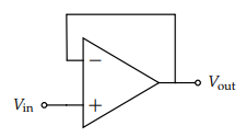 To incorporate negative feedback into our op-amp design, we must create a connection that goes from the output into the negative input
- So when $V_{in} \in [V_{SS}, V_{DD}]$ we get a non-clipped output
- Therefore, it’s common to omit the supply terminals when the op-amp is in negative feedback
- When the op-amp is acting as a comparator (i.e. not in negative feedback) the output voltage is basically always either $V_{DD}$ or $V_{SS}$
- However, when an op-amp is in negative feedback, the output voltage is generally independent of the supply
- We are implicitly stating that the supply voltages are large enough that we never clip
- That is, when negative feedback is applied around an amplifier with high open-loop gain it reduces the overall gain of the complete circuit to a desired value due to the loop gain
- So when $V_{in} \in [V_{SS}, V_{DD}]$ we get a non-clipped output
Checking for NFB #
One convenient method is to check what happens if the output voltage happens to fluctuate by a little bit above the desired output; when this change occurs and propagates back to the input of the op-amp, does it cause the output to come back down to the desired level? If so, the system is in negative feedback.
- Zero out all independent sources as in Thevenin-Norton Equivalencies
- Voltage sources become wires and current sources become open circuits
- “Dink” the output
- If in NFB and $V_{out} \uparrow$, then $U_- \uparrow$ and $U_+ - U_- \downarrow$ (the difference between the higher and lower voltages decreases if the lower voltage increases.)
- Then, $A(U_+ − U_−) \downarrow$ also. From this, we can directly say that $V_{out} \downarrow$
- That is, an increase in the output voltage ultimately led to a decrease in the output voltage.
Golden Rules #
1: $i_- = i_+ = 0$ #
No current flows in/out of the input terminals $U_-$ and $U_+$
- For ideal op-amps, regardless of NFB
- Thus, the behavior of the input terminal’s circuits shouldn’t change
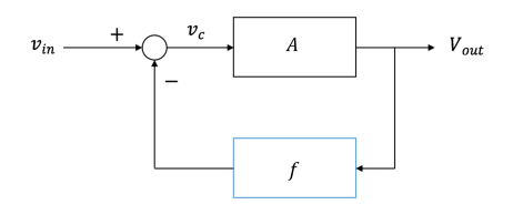
2: $U_- = U_+ \iff$ NFB #
- That is, the voltage potential at the positive input terminal (relative to ground) and the voltage at the negative input terminal (relative to the same ground) are the same
- Intuitively, the “error signal” going into the op amp must be zero
- Implied by $A \to \infty$, full proof on page 7
$$v_{in} - f v_{out} = v_c$$ $$v_{out} = A v_c$$ $$ \Longrightarrow v_{out} = \frac{A}{1+Af}v_{in}$$
Thus, $v_{in} = 0V \implies v_c = 0V$ and $v_{out}$ can be non-zero even when $v_c = 0$ given $A = \infty$
DAC #
Digital-to-Analog Converter: Component that takes in digital signals (bits) and translates them into output analog voltages.
04/07: Buffering, Loading, & Design #
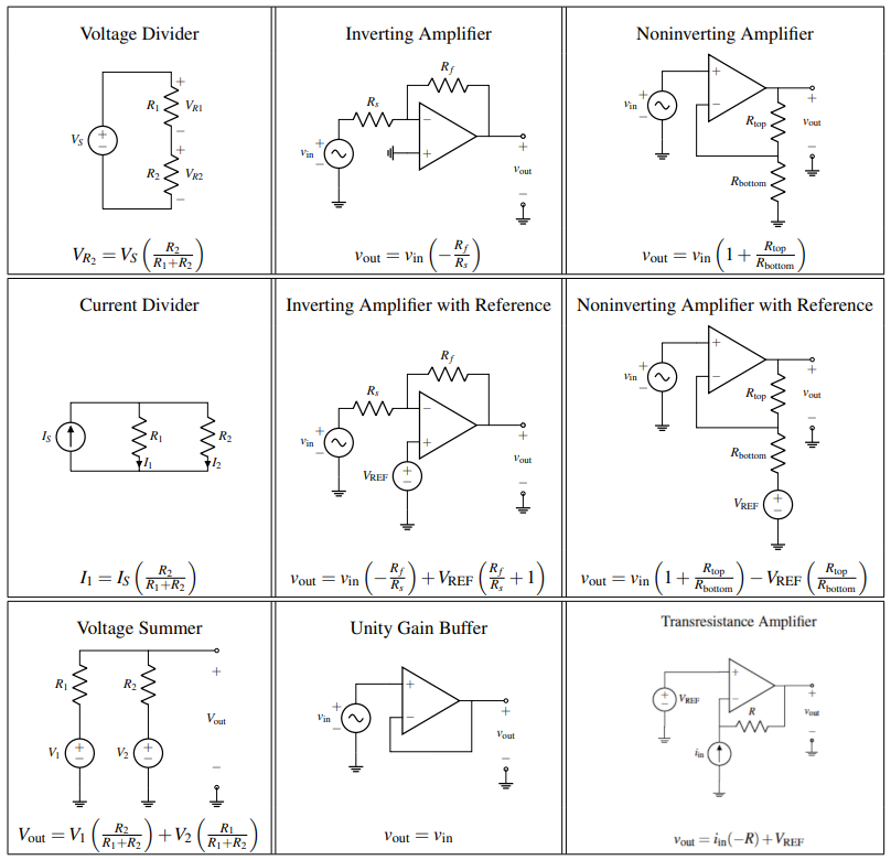
Reference: Op-Amp Example Circuits #
Signals vs. Supply Voltages #
- In real systems, voltages are typically fluctuating signals
- e.x. changes in light intensity or electrical brain activity read from an EEG
- Signals are voltages, they are different from the supply voltages of an op-amp because they are typically much smaller and they change over time
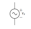
To distinguish, we will use the following symbol to represent time-varying voltage signals:
- Note that while we are alright having signals as our inputs to op-amps, voltage signals generally should not be used for power since they’d create time-varying behavior
Loading #
Loading: an electrical component or portion of a circuit that consumes (active) electric power
- The loading effect makes it hard to design circuits because they mean that components will behave differently depending on what they’re connected to
- Specifically, if the circuit afterwards draws current through some element’s $R_{el}$, then the output voltage drops.
- Furthermore, the amount it drops also depends on the rest of the circuit’s resistance $R_{th}$ – but we don’t want to have to redesign our circuit every time we change $R_{el}$
Example #
- In the real world, the battery (voltage source) has some parasitic, internal resistance along with the wires – $r$
- Thus, the voltage drop across the bulb depends on the value of $r$, which is determined by the battery’s internal structure
- Current flows in this circuit, so some of the battery’s voltage is lost to the internal resistance of the battery
- Most of the time this just means the battery/wires heat up
$$V_{lightbulb} = \frac{R_l}{R_l + r} V_{battery}$$
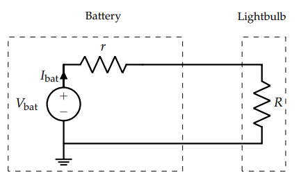
- We want some way to ensure that no matter what $r$ is, the voltage dropped across the bulb was a constant, isolating it from the source
Buffering #
Buffer (amplifier): provides electrical impedance transformation from one circuit to another, with the aim of preventing the signal source from being affected by whatever currents (or voltages, for a current buffer) that the load may be produced with
- Buffers are a powerful tool because they allow us to split circuits into blocks that we can analyze separately and then combine later
- When circuit blocks behave the same way regardless of what they’re are connected to, we don’t need to worry about what’s inside, making it much easier to design complex circuits.
Example #
- We can throw a unity gain buffer in our situation above to solve our issue
- In a unity gain buffer, $v_{in} = v_{out}$
- The voltage at the non-inverting input is $V_{bat}$ since no current can flow into the op-amp (
GR#1) and the same voltage appears at the output because of our unity-gain buffer
- This is the case if, by Ohm’s law, current must flow out of the op-amp– which is perfectly fine since it’s only the inputs that current cannot flow into or out of.
$$V_{lightbulb} = U_{out} = V_{battery}$$
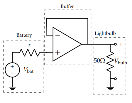
- Now the full $V_{bat}$ will be dropped across the bulb, and we don’t need to worry about any loading effects
- No matter what the $r$ or $R$ values are, the circuit’s behavior is consistent
Design Procedure #
1: Specification #
Concretely restate the goals for the design.
- Frequently, a design prompt will include a lot of text, so we’d like to restate all of the most important features of our design. We’ll refer to these specifications later to determine if our design is complete.
2: Strategy #
Describe your strategy (often in the form of a block diagram) to achieve your goal.
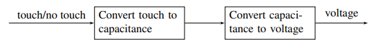
- To do this, start by thinking about what you can measure vs. what you want to know
- For example in our capacitive touchscreen, we want to know if there is a touch and we can measure voltage.
- Since we know that a touch can change the capacitance, we break this down into the following block diagram:
3: Implementation #
Implement the components described in your strategy.
- This is where pattern matching is useful: remind yourself of blocks you know, (ex. voltage divider, inverting amplifier) and check if any of these can be used to implement steps of your strategy.
4: Verification #
Check that the design from 3 does what we specified in 1
- Check block-to-block connections, as these are the most common point for problems.
- Does one block load another block causing it to behave differently than expected?
- Are there any contradictions (ex. a voltage source with both ends connected by a wire, or a current source directed into an open circuit)?